Count on it: Peering at atomic structures with no more than pencil and paper
Who would guess that cracking the mystery of how infinitesimally small atoms arrange themselves at the edges of crystals in advanced materials could be as simple as one, two, three?
Modeling the molecular structure of a crystal’s surface normally requires powerful computers, but University of Wisconsin–Madison engineers have devised a much simpler method — one that’s as easy as counting with pencil and paper.
The simple strategy could help bring about ultrafast computer chips based on materials other than silicon.
“We were surprised to find that it was, in fact, so simple,” says Jason Kawasaki, a UW–Madison professor of materials science and engineering. “With some pretty small tweaks, we could predict structures that were quantitatively very accurate.”

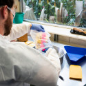
Jason Kawasaki
They were so accurate that his new prediction approach, published June 1, 2018 in the journal Science Advances, offers a quick and easy procedure to zero in on promising materials for use in advanced electronics such as quantum computers that solve problems much more quickly than conventional silicon-based machines.
“Before being able to use materials in interesting ways for next-generation devices, you need to understand how the structure changes at the surface,” says Kawasaki.
Accurately predicting crystal surface structures is a problem that has long bedeviled scientists. Atoms at the edge of a material tend to rearrange themselves, sometimes losing their electronic or magnetic properties.
Kawasaki and colleagues focused on a type of materials called half-Heusler compounds, which have several tunable electronic and magnetic properties. Unfortunately, many half-Heuslers don’t perform as predicted when they are paired up with other materials or pared down to a flat surface.
“When you have little rearrangements of atoms, you can have big changes of properties,” says Kawasaki.
All materials are made up of atoms, which have nuclei at their centers surrounded by ever-shifting clouds of tiny subatomic particles called electrons. Atoms can link up, or bond, by sharing some of their electrons with one another. Crystals consist of many atoms bonded together in a regularly arranged and repetitive pattern. That pattern breaks, however, at crystal surfaces or interfaces, leaving some atoms without partners and unshared electrons dangling away from the bulk material.
Within the rigid interiors of crystals, sophisticated simulations can determine atomic arrangements, but computers need initial best guesses at configurations to create structural predictions.
The simple strategy could help bring about ultrafast computer chips based on materials other than silicon.
For a long time, best guesses at the surface were impossible to come by because the presence of dangling electrons causes the number of possible conformations to skyrocket.
“The right tools and the right theoretical framework didn’t exist,” says Kawasaki.
The right theoretical framework turned out to be surprisingly simple, governed by basic chemistry rules. All that’s needed is to count up all of the electrons each atom brings to the surface, tally all the electrons predicted to be in bonds, and determine if those numbers match. When all electrons are accounted for, the structure is likely to be stable. If not, it’s back to the drawing board.
The counting is so straightforward that Kawasaki can literally use pencil and paper to carry out calculations.
Counting rules are known to work well for simple materials. However, scientists assumed that the electron clouds for the metallic atoms that make up half-Heusler materials were too complicated for such basic accounting.
Kawasaki and colleagues proved that notion wrong.
“We found that a lot of the general rules that have been developed for understanding bonding in simple systems can be mapped onto these more complex materials,” says Kawasaki.
The right theoretical framework turned out to be surprisingly simple, governed by basic chemistry rules.
Using this approach, Kawasaki and colleagues predicted and confirmed the surface configuration for an important half-Heusler material called cobalt titanium antimony, which is a potentially useful semiconductor. The researchers measured the crystal surface with advanced imaging techniques, noting their pencil-and-paper predictions lined up perfectly with real atomic configurations.
The researchers then applied their method to two more half-Heusler compounds, a semimetal and a ferromagnet, and they plan to identify more promising materials.
Kawasaki performed the crystal growth and measurement experiments in collaboration with Chris Palmstrøm, a faculty member in electrical and computer engineering and materials science at the University of California, Santa Barbara.
The research was supported by grants from the Department of Energy (DE-SC0014388), the National Science Foundation (ACI-1053575 and DMR-1121288) and the Wisconsin Alumni Research Foundation.
Tags: chemistry, engineering, materials, research
-
Interwoven
How Indigenous knowledge and science can work together to communicate about climate.
-
UW–Madison’s reach throughout Wisconsin adds up to $38.9 billion a year
The university supports more than 287,000 jobs and helps drive private-sector growth.
-
‘Being part of something bigger than you’ with Badger Volunteers
UW–Madison students head into the local community to find purpose and make a difference.
-
UW–Madison’s Tech Exploration Lab: Where the classroom meets the real world
The lab is built around a simple expectation: Students come to build, test and refine projects with real problems in mind.