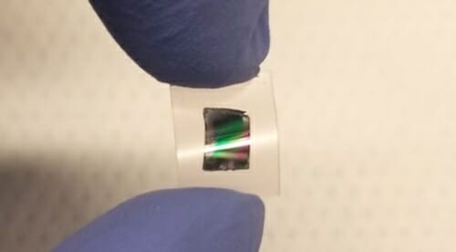
Crystal-stacking process can produce new materials for high-tech devices
The magnetic, conductive and optical properties of complex oxides make them key to components of next-generation electronics used for data storage, sensing, energy technologies, biomedical devices and many other applications.
Stacking ultrathin complex oxide single-crystal layers — those composed of geometrically arranged atoms — allows researchers to create new structures with hybrid properties and multiple functions. Now, using a new platform developed by engineers at the University of Wisconsin–Madison and the Massachusetts Institute of Technology, researchers will be able to make these stacked-crystal materials in virtually unlimited combinations.
The team published details of its advance Feb. 5 in the journal Nature.

To grow layers of single-crystal oxides for electronic components requires neighboring layers to interlock like Lego blocks. A new method throws out that limitation, producing new capabilities for data storage, sensing, energy technologies, biomedical devices and many other applications. Courtesy of Chang-Beom Eom
Epitaxy is the process for depositing one material on top of another in an orderly way. The researchers’ new layering method overcomes a major challenge in conventional epitaxy — that each new complex oxide layer must be closely compatible with the atomic structure of the underlying layer. It’s sort of like stacking Lego blocks: The holes on the bottom of one block must align with the raised dots atop the other. If there’s a mismatch, the blocks won’t fit together properly.
“The advantage of the conventional method is that you can grow a perfect single crystal on top of a substrate, but you have a limitation,” says Chang-Beom Eom, a UW–Madison professor of materials science and engineering and physics. “When you grow the next material, your structure has to be the same and your atomic spacing must be similar. That’s a constraint, and beyond that constraint, it doesn’t grow well.”
A couple of years ago, a team of MIT researchers developed an alternate approach. Led by Jeehwan Kim, an associate professor in mechanical engineering and materials science and engineering at MIT, the group added an ultrathin intermediate layer of a unique carbon material called graphene, then used epitaxy to grow a thin semiconducting material layer atop that. Just one molecule thick, the graphene acts like a peel-away backing due to its weak bonding. The researchers could remove the semiconductor layer from the graphene. What remained was a freestanding ultrathin sheet of semiconducting material.
Eom, an expert in complex oxide materials, says they are intriguing because they have a wide range of tunable properties — including multiple properties in one material — that many other materials do not. So, it made sense to apply the peel-away technique to complex oxides, which are much more challenging to grow and integrate.
“If you have this kind of cut-and-paste growth and removal, combined with the different functionality of putting single-crystal oxide materials together, you have a tremendous possibility for making devices and doing science,” says Eom, who connected with mechanical engineers at MIT during a sabbatical there in 2014.
The Eom and Kim research groups combined their expertise to create ultrathin complex oxide single-crystal layers, again using graphene as the peel-away intermediate. More importantly, however, they conquered a previously insurmountable obstacle — the difference in crystal structure — in integrating different complex oxide materials.
“Magnetic materials have one crystal structure, while piezoelectric materials have another,” says Eom. “So you cannot grow them on top of each other. When you try to grow them, it just becomes messy. Now we can grow the layers separately, peel them off, and integrate them.”
In its research, the team demonstrated the efficacy of the technique using materials such as perovskite, spinel and garnet, among several others. They also can stack single complex oxide materials and semiconductors.
“This opens up the possibility for the study of new science, which has never been possible in the past because we could not grow it,” says Eom. “Stacking these was impossible, but now it is possible to imagine infinite combinations of materials. Now we can put them together.”
The advance also opens doors to new materials with functionalities that drive future technologies.
“This advance, which would have been impossible using conventional thin film growth techniques, clears the way for nearly limitless possibilities in materials design,” says Evan Runnerstrom, program manager in materials design in the Army Research Office, which funded part of the research. “The ability to create perfect interfaces while coupling disparate classes of complex materials may enable entirely new behaviors and tunable properties, which could potentially be leveraged for new Army capabilities in communications, reconfigurable sensors, low power electronics, and quantum information science.”
This research was supported by grants from the Defense Advanced Research Projects Agency (027049-00001) and the Army Research Office (W911NF-17-1-0462).

