Flexible, easy-to-scale nanoribbons move graphene toward use in tech applications

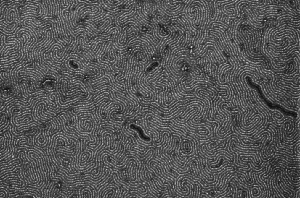
University of Wisconsin–Madison researchers produced the smallest ribbons of graphene yet created, at about 12 nanometers in width, in efforts to use the all-carbon, ultra-thin and adaptable material to improve internet and other kinds of telecommunications performance. The structures, which act like tiny antennas that interact with light, are too small to see with the naked eye. Image courtesy of study authors.
MADISON — From radio to television to the internet, telecommunications transmissions are simply information carried on light waves and converted to electrical signals.
Silicon-based fiber optics are currently the best structures for high-speed, long distance transmissions, but graphene — an all-carbon, ultra-thin and adaptable material — could improve performance even more.
In a study published April 16 in ACS Photonics, University of Wisconsin–Madison researchers fabricated graphene into the smallest ribbon structures to date using a method that makes scaling-up simple. In tests with these tiny ribbons, the scientists discovered they were closing in on the properties they needed to move graphene toward usefulness in telecommunications equipment.\

Joel Siegel
“Previous research suggested that to be viable for telecommunication technologies, graphene would need to be structured prohibitively small over large areas, (which is) a fabrication nightmare,” says Joel Siegel, a UW–Madison graduate student in physics professor Victor Brar’s group and co-lead author of the study. “In our study, we created a scalable fabrication technique to make the smallest graphene ribbon structures yet and found that with modest further reductions in ribbon width, we can start getting to telecommunications range.”
Graphene is hailed as a wonder-material for technologies like telecommunications or solar cells because it is easy to work with, is relatively inexpensive, and has unique physical properties such as being both an insulator and conductor of electricity.
If modified to interact with higher energy light, graphene could be used to modulate telecommunications signals at lightning-quick speeds. For example, it could be used to block unwanted communications frequencies.
One way to improve graphene’s performance is to cut it into microscopic, nanometer-scale ribbon structures, which act as tiny antennas that interact with light. The smaller the antenna, the higher energies of light it interacts with. It can also be “tuned” to interact with multiple light energies when an electric field is applied, stretching its performance further.
The researchers, including teams led by UW–Madison materials science and engineering professors Michael Arnold and Padma Gopalan, first wanted to make a device of graphene ribbons that were narrower than anything made yet. By constructing ribbon-shaped polymers on top of graphene and then etching away some of the surrounding material, they were left with precisely drawn, impossibly thin ribbons of graphene.
“It’s very useful because there are not good fabrication techniques to get down to the feature size we did, 12 nanometers wide over a large area,” Siegel says. “And there is no difference between patterning over the centimeter-scale we’re working with here and giant six-inch wafers useful for industrial applications. It’s very easy to scale up.”
With the devices fabricated, the researchers could then test how the ribbons interacted with light and how well they could control that interaction.
In conjunction with UW–Madison electrical and computer engineering professor Mikhail Kats’ group, they shined different wavelengths of infrared light into the structures and identified the wavelength where the ribbons and light interacted the most strongly, known as the resonant wavelength.
They found that as ribbon width decreases, so does the resonant wavelength of light. Lower wavelengths mean higher energies, and their devices interacted with the highest energies measured yet for structured graphene.
The researchers were also able to tune the ribbons by increasing the electric field strength applied to the structures, further reducing the structures’ resonant wavelength. The researchers determined that one structure has the expected flexibility needed for the technology applications they were aiming to achieve.
They then compared their experimental data to the predicted behaviors of structured graphene across three different ribbon widths and three electric field strengths. The wider ribbons the researchers created closely matched the predicted behaviors.
But for narrower ribbons, they saw a so-called blueshift, or a shift to higher-than-expected energies. The blueshift can be explained by the fact that electrons in the smaller ribbons would be more likely to interact with — and repel — each other.
“The blueshift we observed indicates that telecommunications wavelengths can be reached with much larger structures than previously expected — around eight-to-10 nanometers — which is only marginally smaller than the 12 nanometers structures we made,” Siegel says.
With the eight-to-10 nanometer goal much closer than expected, the researchers are now trying to tweak their fabrication methods to make the ribbons even narrower. These new graphene nanostructures will also allow explorations into the fundamental physics of light-matter interactions, research that Siegel and colleagues are currently pursuing.
This work was supported by the Defense Advanced Research Projects Agency (YFA D18AP00043). SNM-IS (1727523), U.S. Army Research Office (W911NF-12-1-0025 and W911NF-18-1-0149), U.S. Department of Energy (DE-SC0016007), and the Air Force Office of Research (FA9550-18-1-0146).
Tags: materials science, physics


