New computer chip manufacturing method squeezes more onto limited wafer space
Computer chip makers continuously strive to pack more transistors in less space, yet as the size of those transistors approaches the atomic scale, there are physical limits on how small they are able to make the patterns for the circuitry.
Now, taking advantage of a germanium wafer coated with a layer of virtually pristine graphene — a sheet of carbon arranged just one atom thick — a team of engineers from the University of Wisconsin–Madison and the University of Chicago has devised a simpler, reproducible and less expensive manufacturing approach using directed self-assembly.
Directed self-assembly is a large-scale, nano-patterning technique that can increase the density of circuit patterns and circumvent some limitations of conventional lithographic processes for printing circuits on wafers of semiconductors such as silicon.
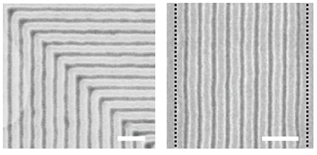
Scanning electron micrographs of block copolymer films assembled on graphene/germanium chemical patterns with 90 degree bends (left side) and with density multiplication by a factor of 10 (right side). The black dotted lines (right side) indicate the period of the graphene/germanium chemical pattern, in which the period of the assembled block copolymer is reduced by a factor of 10 due to density multiplication. The scale bars are 200 nm.
Electrical engineer Zhenqiang “Jack” Ma and materials engineer Michael Arnold of UW–Madison, chemical engineer Paul Nealey of the University of Chicago, and their students published details of the advance in the Aug. 16 edition of the journal Scientific Reports.
Their work could mean a boost in functionality for semiconductor electronics and in capacity for data storage.
To achieve the incredibly tiny size required for the circuitry in future semiconductor electronics, manufacturers are developing directed self-assembly, which enables the fabrication of intricate, perfectly ordered polymer patterns for circuitry.
For directed self-assembly, the researchers use conventional chemical techniques to define a pre-pattern. When chains of molecules known as block copolymers self-assemble on the pre-pattern, they follow the pattern to form well-ordered features.
The researchers’ new method is much faster, and reduces the number of steps in the process to just two: lithography and plasma etching.
In the first demonstration of their technique, the researchers used electron beam lithography and a mild plasma etching technique to pattern one-atom-thick graphene stripes on a germanium wafer. Then they spin-coated the wafer with a common block copolymer called polystyrene-block-poly(methyl methacrylate).
When heated, the block copolymer self-assembled completely in just 10 minutes — compared to 30 minutes using conventional chemical patterns — and with fewer defects. The researchers attribute this rapid assembly to the smooth, rigid, crystalline surfaces of germanium and graphene.
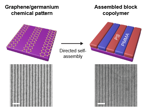
Chemical patterns consisting of alternating graphene and germanium stripes (left side) are used to direct the self-assembly of block copolymers into well-ordered patterns (right side). The top images are schematics and the bottom images are scanning electron micrographs. The scale bars are 200 nm.
Their new method takes advantage of a phenomenon called density multiplication. The researchers used electron beam lithography to first create a larger master template with sparse patterns that guide the orientation of their block copolymers.
When they directed the block copolymer to self-assemble, it did so in a way that enhanced the resolution of the original template — in this case, by a factor of 10. The best previous enhancement by density multiplication was a factor of four.
While the stripe pattern was a simple demonstration of their technique, the researchers also showed it works with more architecturally complex or irregular patterns, including those with abrupt 90-degree bends.
“These templates offer an exciting alternative to traditional chemical patterns composed of polymer mats and brushes, as they provide faster assembly kinetics and broaden the processing window, while also offering an inert, mechanically and chemically robust, and uniform template with well defined and sharp material interfaces,” says Nealey.
The technique enables them to combine the uniformity and simpler processing of traditional “top-down” lithographic methods with the advantages of “bottom-up” assembly and greater density multiplication, and offers a promising route for large-scale production at significantly reduced cost.
“Using this one-atom-thick graphene template has never been done before. It’s a new template to guide the self-assembly of the polymers,” says Ma. “This is mass-production-compatible. We opened the door to even smaller features.”
The researchers are patenting their method through the Wisconsin Alumni Research Foundation. Funding from the U.S. departments of Energy and Defense, UW–Madison and the University of Chicago supported their work.
Other authors on the paper include Tzu-Hsuan Chang, Robert M. Jacobberger, Solomon Mikael, Dalong Geng and Xudong Wang of UW–Madison, and Shisheng Xiong, Hyo Seon Suh and Chi-Chun Liu of the University of Chicago.
Tags: electronics, nanotechnology, semiconductors, WARF
-
UW–Madison again named a ‘new Ivy’ by Forbes
The university was selected as one of the best in the country at "preparing and graduating the talent" that meets today's workforce needs.
-
UW–Madison graduate programs ranked among the nation’s best by U.S. News
Nearly 20 programs ranked in their respective Top 10 lists, shining a light on the breadth and depth of the university’s graduate offerings.
-
UW–Madison students ‘step into the professional world with a purpose’
More than 90% of UW graduates say their education prepared them for their career, according to new survey results.
-
How UW–Madison and industry are working together to shape Wisconsin’s AI future
As businesses explore how to apply AI effectively and responsibly, UW researchers, faculty and students are offering their knowledge in the emerging space.